After almost a century, in 2004, researchers have succeeded to fabricate field effect device based on single layer graphene which is a truly one-atom thick highly conductive sheet. It turns out that graphene is a member of a much broader family of materials, named van-der Waals (vdW) 2D materials, in which the chemical bonds within the 2D planes are much stronger (covalent bonds) than those between the 2D layers (vdW bonds). This property makes it possible to peel single 2D plane out of a 3D bulk material without breaking the integrity of each sheet. As a consequence, similar to the standard periodic table which arranges the chemical elements according to their chemical and physical properties, a new 2D periodic table has emerged. The new table contains semi-metallic and metallic 2D materials (graphene family, and transition metal dichalcogenides family (TMDs)), 2D insulators (hexagonal boron nitride (hBN)), 2D semiconductors (TMDs family, black phosphorous family, III-VI family), and even superconductor 2D materials (TMDs family).
Since these materials are truly 2D, meaning a single crystallographic unit cell thick, it is possible to stack them together without being limited by crystallographic matching between adjacent material layers. From a physics point of view, it means that two such layers are not necessarily in thermodynamic equilibrium but yet are stable (i.e., metastable state with infinite lifetime). Namely, the new 2D periodic table can be used to create a variety of synthetic composite materials which were not accessible so far. Moreover, as crystallographic matching is not an issue, it is also possible to assemble different layers with defined twisting angle between them. This new degree of freedom enables the formation of homo- or hetero structures with different symmetries, band structures, and physical properties. A remarkable example was found recently where superconductivity of twisted bilayer graphene was reported with similar behavior as high-Tc superconductors.
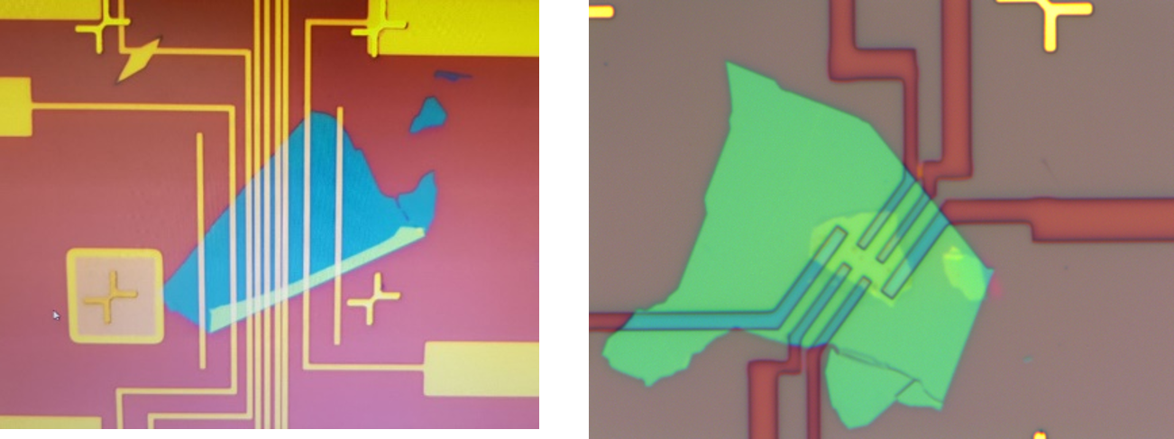
Our group integrates one dimensional (1D) materials, such as carbon nanotubes (CNTs) and silicon nanowires with this new class of 2D materials for realizing novel and unique electronic structures and devices. We study the electrical and mechanical coupling between 1D and 2D materials, and address both basic science and technological applications based on these materials. Specifically, we study the following topics:
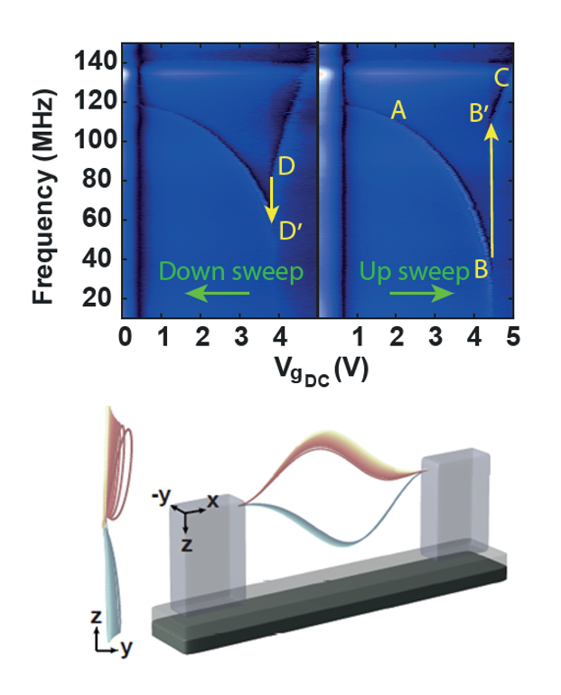
- We utilize mechanical resonators from these materials and study dissipation phenomena at the nano scale, non-linear behavior, mode mixing, and mechanical qubit for quantum research.
- Artificial atoms (quantum dots) embedded within 1D and 2D heterostructures.
- Tunneling physics between different materials and dimensions.
- Charge and Spin transport within low D materials for classical and quantum electronics.
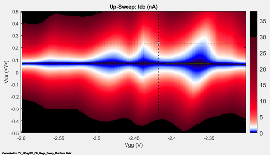
- Non-volatile memory cells, memristors, and atomristors based on 1D and 2D materials.


